- Sign In
-
Join Free
New here? Get your coupons!
- Sitemap
-
My PCBAStore
Add: Building E, No.58, Nanchang Road, Xixiang , Baoan District Shenzhen City, Guangdong, China
Tel : 0755-27348887
Fax : 0755-27349876
E-mail : svc@pcbastore.com
Simon / 2021-04-09
Contents [hide]
Just like the name suggests, stackup refers to the collection of copper and insulator layers that create a PCB before coming up with the final design of the board. There is a need for compacted electronic products, and that is why PCB layer stackup is pivotal in the electronics world. For electronic products to have that compacted design, designers see the need of putting up PCBs that contain multiple layers and a 3-dimensional outlook on the design. The multiple layers help with the following: increasing the capability of the board to distribute energy, supporting signals with high speed, eradicating electromagnetic interference, and minimizing cross-interference.

There are fundamental differences between standard stackup and HDI stackup. For standard stackup, there are factors to take note of including: progression of layers, the quantity of the layers, circuit's frequency, and requirements regarding emission. Other parameters related to standard stackup include: the space between the layers and shielded or unshielded area.
Of great importance still, are the design rules that are important for standard stackup. The rules include: maintaining the space between the layers of signals and using large cores to evade EMC issues. Another thing that is significant to note is the benefit of standard stackup, which is guarding of inner layers using the planes on the exterior layers. The disadvantage is the lessening in the ground plane as a result of the presence of component mounting pads, specifically on a PCB with high density.
HDI stackup is the technology that is transforming the manufacturing and design of multiplayer PCB. Unlike the standard stack up, HDI stackup offers more design choices. Additionally, if you would like to have a simplified design for complex boards, HDI stackup is the right choice. The factors that determine stack up include: the quantity of signal layers and the quantity of ground and power layers. An important thing to take note of is that the layers should have a symmetrical arrangement. The fact that HDI does not need complicated architectures is a big plus for designers.
Just like it is for any other design or product manufacturing, there are rules that designers should follow in order to produce products with the best quality. If you're not going to invest in the best, the likely outcome is poor products. As you already know, electronic products go through processes and involve different components before the production of the final product. Therefore, it is important for designers to ensure that they identify and follow the proven best practices of designing PCB stackup. For PCB stackup design, there are rules that one should put into consideration in order to have the best possible outcomes.
The first rule is the usage of ground plane boards. They are the best to use because of their ability to permit signal routing in stripline arrangement. Moreover, it plays a vital role in reducing ground noise. The ground noise reduces significantly as a result of reduction in ground impedance.
In regard to high-speed signals, they have to be routed on intermediate layers placed between the different levels. Through this, ground planes play the role of a shield and contain the radiation emanating from the tracks at top speed.
It is also important to ensure that the layers of signal are in close proximity to each other even in adjoining planes.
A signal layer has to be close to a plane
The power and mass planes should be meticulously joined together
Make sure that the configurations are symmetrical
You should work towards improving EMI performance and also reduce noise
It is also imperative to put into consideration the thickness of every signal layer
Additionally, it is vital to put into consideration the properties of the materials required. Take note of the thermal, electrical, and mechanical properties of such materials.
You should also consider the software to use when designing the stackup.
Excellent PCB design carries a great deal of significance. It is a great necessity for you to have a quality product and outcome. As you probably know, circuits today operate at very top operating speeds, thus making it extremely necessary for PCB design to be at its best. The need for proper PCB design is making the process to be regarded as an art. The reason for this is because you can either come up with a good or a poor design. The truth of the matter is that a PCB with a poor design can damage or affect the performance of an electronic product. These are some of the effects of a poorly designed PCB: poor signal submission, low quality power delivery, and reduced durability of electronic products. In order to avoid the above-mentioned effects, it is highly advisable for one to ensure that a printed circuit board has a high-quality design.
The final design of your board is essential. The design you come up with will determine the performance of the final product. For you to have a quality PCB stackup design, here are valuable tips you should put into consideration:
The first tip is for you to ascertain the number of layers. You should be aware of the quantity of layers that you need for the PCB stackup. This requires for you to put the following into consideration: power, signal, and ground layers. You can also consider planes. For the signal, you can consider either high or low speed. Electrical experts advice that you should not blend signal types on interior layers. For you have a precise layer count, you can make use of pin density. This is applicable for most boards.
Secondly, ascertain the layer arrangement. Once you have known the number of layers you need, the next thing is to ascertain how the arrangement will be or how the stackup will be. The rules to follow in this stage include:
Position signal layers close to inner power layers for the sake of tight coupling
There should be minimal space between power and ground layers
Make sure that 2 signal layers are not adjoining to each other
Ensure that the stackup has a symmetrical arrangement
Thirdly, decide on the materials of the layers. An essential factor to put into consideration for your PCB stackup is the thickness of every signal layer. A good tip for you to use when selecting the materials is the thermal, electrical, and mechanical properties of the materials. They should help you make the right decision concerning the materials to use.
Lastly, get to know the PCB routing and vias. For your PCB stackup design to be complete, you have to determine and route the traces. This process includes the following: ascertaining copper weights, the place to position vias and the kind of vias to apply.

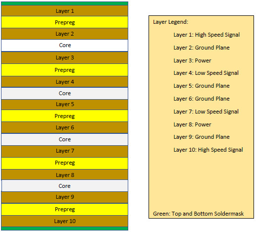
Above is an example of a PCB stackup design. It is possible to various stackup designs depending on the way a designer chooses to implement the above-mentioned tips.
PCB stack up designs are important for electronic engineers and designers. The ability to come up with a good-quality electronic product takes a lot of things into account. Without a quality electronic product, the quality of the product and its performance will be affected greatly. That is why it is important for designers to ensure that they put together the required components and materials in order to get quality products. PCBs are among the most important electrical components that are required to run an electrical product in the best way possible. In the same way, there are different components that are supposed to be in a printed circuit board for it to run effectively. Of greater importance is the design of a printed circuit board. The stackup design of PCB carries a great deal of significance in determining how it performs.
A quality flex PCB stackup design goes a long way to maximize the output and productivity quality of a PCB. The Standard stackup and HDI stackup designs are commonly used by designers when designing PCB stackup designs. Both designs have unique features and advantages that attract designers and engineers to them. You can use the one that suits you best depending on the design you want and the kind of performance that you would want to see from it. An important aspect to put into consideration is that there are best practices that you should consider for you to have a properly designed PCB stackup. Like any other production or creation, it is possible to have a poor PCB design. That is why it is of great significance to follow the rules of PCB design in order to come up with the best electrical products. Remember, the quality of a PCB stackup design determines electrical products function and perform.