- Sign In
-
Join Free
New here? Get your coupons!
- Sitemap
-
My PCBAStore
Add: Building E, No.58, Nanchang Road, Xixiang , Baoan District Shenzhen City, Guangdong, China
Tel : 0755-27348887
Fax : 0755-27349876
E-mail : svc@pcbastore.com
Luna / 2020-11-09
Contents [hide]
A PCB Gerber file for each section of your electronic circuit design is what you need if you want to create a PCB. In order to ensure delivery time and reliability of end products, PCB design engineers should learn how to generate PCB Gerber files on their own. PCB Gerber files generally contains design data of signal layer, soldermask layer and silkscreen layer.
Nowadays, there are three versions of Gerber formats available:
• Gerber X2 - the newest Gerber format with stackup data and attributes contained.
• RS-274-X - an expanded version of Gerber format and it has been widely applied.
• RS-274-D - the oldest version of Gerber format which is being gradually replaced by RS-274-X
Different PCB design software feature different operation steps of PCB Gerber files generation. In the following part of this article, We will show you how to generate PCB Gerber file from Cadence Allegro in details.
Open your PCB layout in Cadence Allegro:
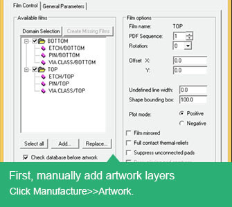
1. First, manually add artwork layers, and then click Manufacture>>Artwork.
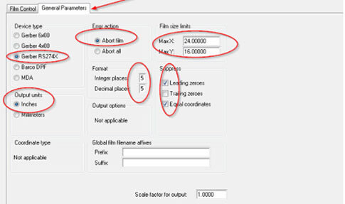
2.Click General parameters, setting as shown below:
3.Then click Film Control,add artwork layers, add a board outline by right-clicking on the TOP folder and picking Add Manual.

4. Determine a film name, OUTLINE for example and click OK button.

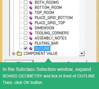
5. In the Subclass Selection window, expand BOARD GEOMETRY and tick OUTLINE. Then, click OK button
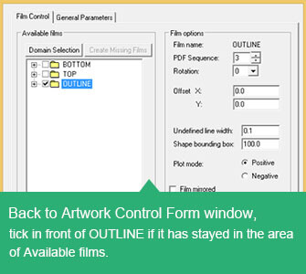
6. Back to Artwork Control Form window, tick OUTLINE if it has stayed in the area of Available films.
7. Use the same method to add other layers, Assembly layer is similar to the picture below

All the signal layers are set similar to the picture below:
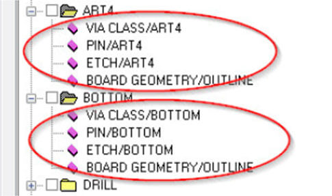
Drill layer is set similar to the picture below:
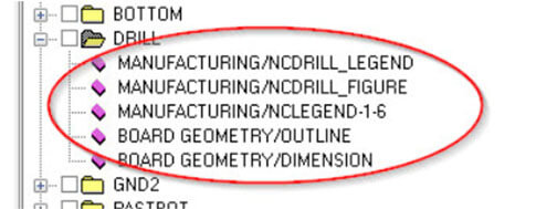
Silkscreen layers are set similar to the picture below:

Paste mask layers are set similar to the picture below:

Then setting and output the drilling file
1. Add the drilling table
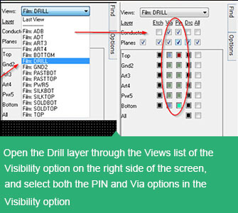
Open the Drill layer through the Views list of the Visibility option on the right side of the screen, and select both the PIN and Via options in the Visibility option, as shown below:
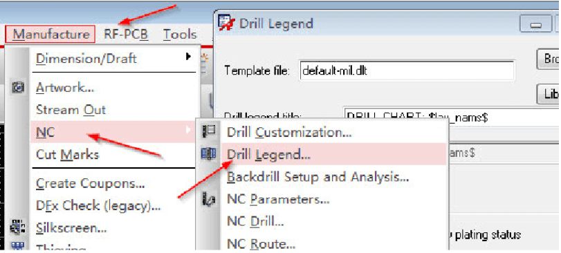
Then click Manufacture>>NC>>Drill Legend, as shown below:
The drilling table parameters are setting as shown below:
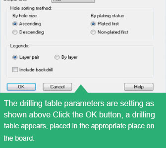
Click the OK button, a drilling table appears, placed in the appropriate place on the board.
2.Output the drilling file
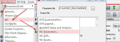
The parameters are setting as shown below:
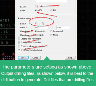
Output drilling files, as shown below, it is best to click the dirll button to generate .Dril files which means drilling files
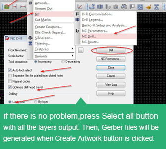
With these steps finished, you need to re-confirm whether each parameter is set correctly, if there is no problem,press Select all button with all the layers output. Then, PCB Gerber files will be generated when Create Artwork button is clicked.
If you have any comments or suggestions about this post, please leave a reply here or contact us and we will do our best to assist you!