- Sign In
-
Join Free
New here? Get your coupons!
- Sitemap
-
My PCBAStore
Add: Building E, No.58, Nanchang Road, Xixiang , Baoan District Shenzhen City, Guangdong, China
Tel : 0755-27348887
Fax : 0755-27349876
E-mail : svc@pcbastore.com
Byron / 2020-12-13
Contents [hide]
PCB is normally showed as single Piece in drawing after design, and make it as single piece in the production as well, However, many electronics engineers new to PCB industry don’t really know how and why to design and manufacture their PCBs in a panel array, and their manufacturing partners may not tell their more about production processes and pricing model of panel production.
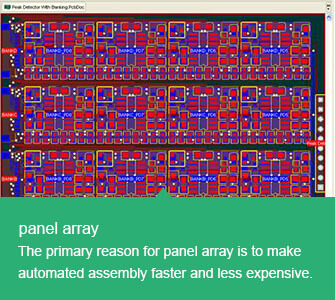
The primary reason for panel array is to make automated assembly faster and less expensive. Running an array of boards through a pick-and-place machine is far more efficient than sending them through one at a time. Arrays are also desirable because they allow the addition of tooling rails, tooling holes, and fiducials, all of which help your assembler.Because usually PCB assembly process require panelized PCB to improve efficiency, and if the PCB board is special small with irregular outlines, this will be difficult for PCB manufacturing process as single piece, we need to panelize these PCB before production, which will be helpful to shorten PCB manufacturing lead time, it will be also easy to control quality and count PCB quantity before shipment.

1.Panel Design with break-away but without spacing between each single piece, this is the most common way, generally, it is popular to most customer if customers do not have special requirements on PCB outline and PCB bur after profile, normally use V-cut to separate the PCB boards as single piece, but sometimes these single piece will have slight bur, but it's also easy to polish the bur and will not influence PCB function, on the other hand, the break-away is helpful for the boards to fix on the machine and strengthen the whole array.
2. Panel Design with break-away, and spacing between each single Piece. If customers have special requirements on PCB outline and board edge without bur existing, in that case we have to use the profile of routing, thus, it requires spacing between each single board, generally the spacing is within 1.5~2mm, This will be helpful to control the bur.
3. Panel Design without break-away, which is convenient for shipment, but not helpful for follow-up process, there are a few customers need to do assembly by manual, if so it's feasible to use Panel Design without break-away, this kind of Panel Design will save the cost for board edge and make cost down properly.
4. Panel Design with stamp holes, the stamp hole is the small holes to connect single boards, these holes look like stamp saw tooth, so it's called stamp hole connection.PCB manufacturers could use stamp hole connection to control and reduce burs, so the stamp holes can be used to replace V-CUT.
Except the types of panel design above, There are more methods for panel design, If you want to know more about it if you want to know which type is the best for your PCB projects. PCBASTORE will give you the complete solutions
If you have any comments or suggestions about this post, please leave a reply here