General, quoting & support.
Add: Building E, No.58, Nanchang Road, Xixiang , Baoan District Shenzhen City, Guangdong, China
Tel : 0755-27348887
Fax : 0755-27349876
E-mail : svc@pcbastore.com
PCB Copy Board Methods And Procedures
fannie / 2017-11-18
Contents [hide]
First,get a PCB, first recorded on paper all the good vitality of the model parameters, and the location, especially the direction of the diode, three machine direction of the tube, IC notch. Preferably with a digital camera to shoot two photos vitality location.

Second, to remove all the devices, and the PAD hole in the tin removed. PCB clean with alcohol, and then placed in the scanner, start POHTOSHOP, color printing mode to sweep the surface, and print them out for use.
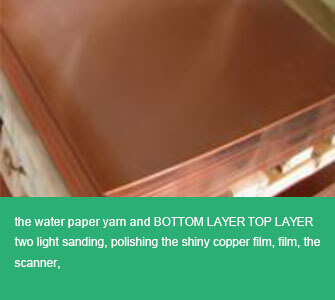
Third, the water paper yarn and BOTTOM LAYER TOP LAYER two light sanding, polishing the shiny copper film, the scanner, start PHOTOSHOP, the two-color mode, respectively sweep. Note, PCB placed in the scanner must be horizontal tree straight, otherwise the scanned image can not be used.

Fourth, adjust canvas contrast, brightness, contrast so that some portion of the copper film and a copper film not strong [industrial electrical network -cnelc], and then the second drawing to black and white, check the line is clear, if not clear, repeat this step. If clear, the map as black and white BMP file format and BOT.BMP TOP.BMP
Fifth, the two BMP file formats are converted PROTEL format files transferred in PROTEL in two basic positions coincide as over two-PAD and the VIA, indicating that the first few steps to do well, if there is deviation , the third step is repeated.
Sixth, the TOP. BMP into TOP. PCB, pay attention to the conversion to the SILK layer, that layer is yellow, then you are in the TOP layer scanning lines it wants, and in accordance with the second step of drawing placement device. After drawing the SILK layer deleted
Seven, the BOT. BMP into BOT. PCB, pay attention to the conversion to the SILK layer, that layer is yellow, then you line it wants in the BOT layer description. After drawing the SILK layer deleted.
Eight, in PROTEL in TOP. PCB and BOT. PCB transferred, combined into a map on it, so PCB copy board is complete
Hope above information will helpful for you to finish PCB Copy!
If you have any comments or suggestions about this post, please leave a reply here or contact us and we will do our best to assist you!
Previous article:What are PCB Test Jigs, PCB Test Fixtures and How to Test PCB?


