General, quoting & support.
Add: Building E, No.58, Nanchang Road, Xixiang , Baoan District Shenzhen City, Guangdong, China
Tel : 0755-27348887
Fax : 0755-27349876
E-mail : svc@pcbastore.com
What Is PCB Solder Mask?
Simon / 2021-02-18
Contents [hide]
What Is Solder Mask?
PCB encompasses layers of copper, which provide the ground of printed circuit boards. Soldering is employed on every component of the PCB by a soldering machine. The connection of these components occurs within the copper traces. After that, a film that secures these components is supplied on the traces. This is done on either side, which is best referred to as the solder mask.
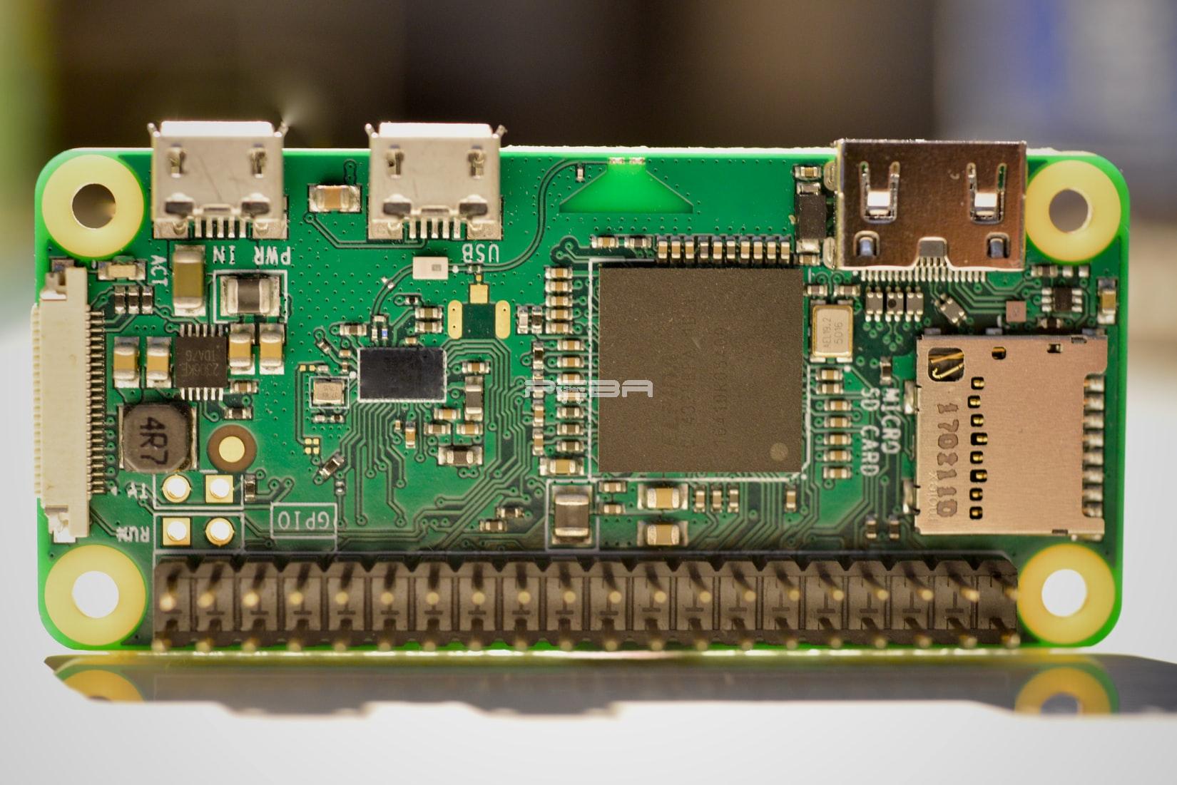
In simple terms, a solder mask, also termed as solder stop or solder resist is a thin protective layer of polymer used on PCB copper traces to hinder the oxidation process that can be initiated when exposed to air or environment. This also helps to secure copper from impurities such as dirt and dust.

A solder mask is also essential in allowing designers to attain great soldering easily. This is due to the reduction of the possibilities of solder bridges developing in nearly-spaced solder pads. Wondering what solder bridge entails? Well, it is a link that forms in two conducting sections of the PCB board via unintended blob, small and whisk.
It is not always a must that you will get solder resist or mask on hand-assembled PCB circuits; however, they are critical elements for several produced boards that require automatic soldering utilizing reflow or solder-bath methods. Furthermore, when solder resist is applied to the electronic design elements, it is used as a unique PCB layer that looks the same as silkscreen and copper layers.
Different Types of Solder Mask
There are several types of solder mask PCB. Below are the most common;
1. Epoxy liquid
This is a popular kind of solder mask, which is most loved because it is cheap. Being a polymer kind of thermosetting, epoxy liquid is normally silkscreened on the pattern of the PCB board. The method of silk screening employs a woven mesh, which props stencils or ink-blocking sequences. Transferring ink is done via open sections generated by the mesh. The silk and synthetic fiber are pondered for that reason. Notwithstanding, ink is the primary option since synthetic fibers are considered for electronic applications. The last stage in this type of solder mask occurs when performing thermal curing.
2. Dry film photoimageable
In this kind of solder mask, a thin layer is applied to utilize a vacuum lamination. The mask is uncovered after the application. Uncovering means that the layer is exposed, which implies that several openings are generated in the sequence while soldering the parts to the pads. A layer of copper is introduced into the trace sections, including inside the holes via a technique referred to as electrochemical processing. Technically, tin is introduced on the trace of copper to safeguard them from the oxidation process. Once soldering masking is over, there is the removal of dry film, leading to the exposure of the etched copper area. During the final process, the finishing is carried out via thermal curing.
3. Topside and bottom side masks
Solder masking on the top is essential as it offers electronic engineers easy accessibility to the holes available in the green solder stop that is included to the PCB board by film, ink, or epoxy method. Element pins can as well be soldered to the PCB board employing those recognized areas. The sequence of the copper traces on the upper side of the board is referred to as the top traces while those on the lower side of the board specifies the openings.
4. Liquid ink photoimageable
Technically, a liquid photoimageable solder stop is employed as the ink shaping. This implies that the ink is silkscreened or just sprayed on the board. After that, liquid ink is uncovered to the sequence. In most cases, the analysis of the liquid ink is carried out using HASL. Hot air surface leveling is basically a method that requires a neat working environment, free from particles and other impurities. The next step is exposing the board to the UV light, which assists in drying the film. Removal of the mask follows employing developers. These developers are normally water sprays that come at high pressure. The last stage here encompasses organic coating plus thermal curing.
These are just some kind of PCB solder masks available. If you are not sure of the right option to consider for your electronic applications, it is recommended to get in touch with the company expert. The reason for approaching these experts is that they are experienced in PCB manufacturing.
What Are the Solder Mask Processes
The process of solder masking includes many steps as follows:
1. Pretreating
It can be a daunting task to connect the solder and copper layer; in case the copper had undergone oxidation or rather it is too smooth. To help avoid this issue, copper is pretreated prior to coating commence. Preheating helps degrease the oxidized layer.
2. Coating
Coating, also known as screen printing is done to give the solder mask color based on the customer's requirements to the PCB board.
3. Drying
After coating, drying is fostered for about 15 minutes prior to pre-baking. This assists in minimizing pre-baking work by the process called solvent evaporation.
4. Pre-baking
The process of pre-baking is to continue evaporating the solvent ink in the tunnel oven. The temperatures of pre-baking, ventilation management and time control are such great aspects. Note that progressive pre-baking can lead to issues in development.
5. Registration
This is done after pre-baking and normally happens with film,
6. Exposure
Prior to exposing the latter, kindly confirm if the glass frame and polyester film based on the exposure film are neat or not. After confirmation, switch on and open the vacuum area to choose the exposure program.
7. Developing
This is getting rid of the solder solvent that is actually found on the pads in shading sections. This is easily done by sodium carbonate in a 1% concentration. The temperature of the liquid is normally 28-32 degrees Celsius. Prior to full developing, developing machine temperature should be improved so the solution can attain a reasonable temperature and foster developing effects.
8. Inspection
Inspection is required to confirm if burrs and defect images are available and removed.
9. Final curing
The right PCB board should be placed on the tunnel oven to foster baking and promote the last thermal curing. You may require UV curing sometimes to boost the mechanical and chemical characteristics of the solder stop.
How the Solder Mask Process Affects PCB
Not that you contemplate the whole process of solder stops or solder mask, let us delve into how this process influences PCB.
1. Solder bridge prevention
It creates a solder dam between copper sections and solder joints. This leads to the development of a solder bridge that is potentially known to cause board damage and short circuits.
2. Low rate of solder paste usage
It enables minimal solder paste in the soldering process.
3. More insulation to the PCB components
It acts as an insulator of the PCB elements.
4. Safeguard the PCB board
It helps avoid oxidation of the copper traces that may influence the running time of the electronic device. It also protects the board against dirt and other elements.
5. Enhances the voltage of breakdown
An increase in the voltage breakdown will help offer extra security against arcs primarily linked to high voltage.
Solder Mask Design Tips
Solder stop and/or solder mask is can be pondered unnecessary in PCB manufacturing; however, without employing it will lead to many issues that can highly minimize the lifespan of the board. Therefore, when designing PCB boards using solder mask, it is important to consider the following tips;
1. The thickness and the type of the solder mask
Selecting the right solder mask relies on some aspects such as the surface, layout, conductors, dimensions of the board, and the components. If you are developing components for fields like telecommunication, medicine, or aerospace, the solder mask you select must have specific standards. Basically, liquid photo-imageable options are the right and commonly used due to their reliability, low price, and ability to create good contact with the PCB board's surface.
Primarily, solder mask thickness relies on the width of traces used on the board. In most cases, approximately 0.5 mils solder masks are used on the copper. When using a liquid mask, it will normally offer a distinct thickness. This can go up to 1.2 mils thick and 0.3 mils thin. Learn more about PCB thickness details here.
2. Know how to include it in your design
The design of the PCB board demands that the mask be utilized as the Gerber file layer. These are basically negative images implying that the colored sections are the ones not engulfed by the mask. Simply put, the file will portray the areas not necessary to apply the mask.
Therefore, the rule of the thumb is to engulf the whole PCB board with solder stop, while leaving the sections your elements or components will fit. You can also leave the spaces for test points.
3. Avoid relief issues
Relief areas of the solder mask normally border surface-mount pads via the test points, hole pads, and vias as error margins during the fabrication process. However, the space of the solder mask formed between two adjoining relief is considered the solder stop dam. The measurement of this solder stop dam relies on the resolution of the mask.
Conclusion
A solder mask or solder stop can be employed for both automatic and hand assembly. It is a crucial technique in the whole PCB fabrication process. Indeed, for improved performance and efficient connection, a solder mask will help avoid copper trace oxidation, hinder unexpected connection, and keep dirt and dust at bay.


