- Sign In
-
Join Free
New here? Get your coupons!
- Sitemap
-
My PCBAStore
Add: Building E, No.58, Nanchang Road, Xixiang , Baoan District Shenzhen City, Guangdong, China
Tel : 0755-27348887
Fax : 0755-27349876
E-mail : svc@pcbastore.com
Alina / 2018-01-09
Contents [hide]
You're probably wondering what can go wrong, here are some of the influences of not making final silkscreen adjustments before sending off your design.

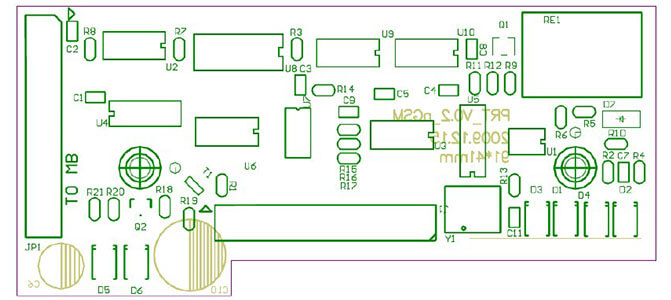
Misrepresented components: If a silkscreen doesn’t accurately represent its intended components, it can lead to confusion for the technicians doing debug or modifications. This can include a shape that incorrectly represents the associated component or pin numbers and polarity indicators that are on the wrong pins. You can imagine the sort of angst that board technicians will feel when they are probing for the plus side of a cap and find out that the polarity indicators are actually reversed.
Un-readable silkscreen text: If the silkscreen text is unreadable it takes the board technicians more time to interpret the reference designators. This is often due to using too small of a font size to be legible or using the wrong line width size. Line widths that are too narrow won’t screen print on the board successfully while line widths that are too large will balloon and become equally unreadable.
Reference designators placed on wrong components: Sometimes the reference designators end up on the wrong components. This can happen if a component is moved but not the reference designator, or it can be an error on the part of the designer. In any event, the board technicians trying to test the board will end up probing components that don’t match what they see in the schematic.
Reference designators are covered by assembled components: We’ve also seen plenty of examples where silkscreen reference designators end up under assembled parts. This is sometimes unavoidable in dense designs, but we should do our best to not let it happen. Again, the board technicians will struggle to find “C143” on your design when the reference designator isn’t visible.
Silkscreen ink covering metal or going into holes: Silkscreen ink that ends up covering bare metal, such as surface mount pins or plated thru-holes, can actually cause a board to be scrapped. As well, silkscreen elements that collide with other silkscreen elements or silkscreen that end up off the edge of the board don't help anyone.
The first step in avoiding these kinds of errors is to become familiar with your circuit board fabricator’s silkscreen design guidelines. They will give you information on the optimum and minimum font sizes and line widths. They will also be able to give you clear specifications for silkscreen to other objects, including bare metal and plated thru-holes. Establishing good communication with your fabricator and understanding what they need before you submit a design to them is an essential key to reducing manufacturing errors.
Look at your design with a fresh pair of eyes, as if you were the one responsible for modifying and debugging the board. If you can view the output of your design’s silkscreen through a separate viewer it will help with this check. Can you see and read all of the reference designators? Do you have large pin-count parts marked in order to find pin 1? Do you have the correct polarity indicated on the appropriate parts? If you can’t read and interpret the silkscreen, then be assured that your technicians won’t be able to either.
Finally, use the Silkscreen DRC’s in your CAD system. Make sure to check for silkscreen over bare metal, silkscreen going into holes, and silkscreen clearances to other objects and other silkscreen elements. These checks can save you from a lot of grief.
Let’s face it; designing a board can be a lot of fun. In fact, the final hand routing can be very cathartic, especially after completing a challenging place and critical route. Nevertheless, the design has to be prepared for the final output files and that can be a tedious and monotonous task. It is not uncommon for PCB designers to give silkscreen clean-up and other output related tasks less than their full attention because they just want to be finished with the design and move on to the next project. But like an Olympic gymnast, you have to finish strong.
If you have any comments or suggestions about this post, please leave a reply here