General, quoting & support.
Add: Building E, No.58, Nanchang Road, Xixiang , Baoan District Shenzhen City, Guangdong, China
Tel : 0755-27348887
Fax : 0755-27349876
E-mail : svc@pcbastore.com
What Is PCB Stencil?
Simon / 2021-01-28
Contents [hide]
What is PCB stencil? What are the procedures to make a PCB stencil? What are the proven ways for cleaning PCB stencil? So, you have these doubts in your mind. You want to be armed with the required information. The following article will clarify all your doubts.

What Is PCB Stencil?
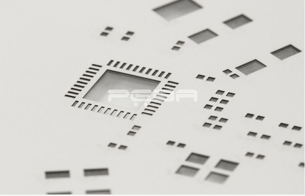
You might be aware that a stencil is a thin material sheet that bears the structure of apertures. It determines the component's layouts on PCBs. The benefit of the solder stencil is that it can be used to deposit the exact solder paste quantity while maintaining precision across the board.
After applying the solder paste over the PCB, the board will become a set for installing SMD. The deposit of the solder paste will sit on the board depending on the apertures of the stencil after removing the stencil. The perfect deposition of the paste will make sure that the joints are the best concerning electrical connections as well as mechanical strength.
In the current condition, suppliers of PCB pads are also showing interest in producing PCB stencils. You can go with custom made designs as well. There will be two types of stencils. One is frameless and the second is framed. If you are looking for a cheaper option, you can go with the frame-less type. It is affordable and easy to store as well. You can use them for the high volume printing. Frame-less type is considered the second-best for high volume printing.
If you want, you can consider adding a stencil to PCB fabrication orders. All you need to do is to place a PCB order in a normal way. You will have the option to choose from different stencil sizes and types. However, make sure that they complement each other.
When it comes to the design, you can expect many. There are stencil thickness, aperture design, alignment, and PCB-specific design. In some cases, the PCB pad might require varying thicknesses. Some might need thin stencils.
How to Make PCB Stencil
In the PCB assembly, the printing phase is the most difficult one. It demands careful attention. A minor mistake can ruin all your effort. So, careful observation is needed to avoid such a condition. In most cases, the error comes from the mounting of the solder joints. The PCB stencil will enable users to mount all the joints on the PCB board. They can mount all the solder joints in one go. What will happen if you can mount all the joints in one go? It will save a lot of time and energy. Also, if they do it right, they can minimize the possibility of any error. Here are the steps to make you fully aware of the entire process.
Step 1: Stack the Sheet
Start the process by stacking two Mylar sheets together. During the process, you will have to first heat the Mylar sheets. Heat the sheets to detach them from the stack. While doing so, the second sheet is going to absorb the first sheet's melted pad. It will enable the first sheet to be cleanly pulled off.
Step 2: Export from the ExpressCAD
You can consider either EagleCAD or ExpressCAD. If you are using EagleCAD, you need to export the bottom and top cream layers via the cam file. When you are using the Express PCB, you will have to open the File menu. After opening the file menu, you just need to select Export DXF Mechanical Drawing. If you want to download PCB CAD softare, check here.
Step 3: Swell Pads
When you have software that can export PCB Gerbers, you will have to recompense for melting. As the melting will increase the pad size, you will have to act smart to cut down the size to get the required size. You might be thinking that how to do this. It is simple. First, you will have to select the file, import, and Gerber for importing the cream layers into the ViewMate. After this, you need to select setup, and then D Codes. You need to select all the columns in the given area and then you will have to open Operations and then �Swell'. Make the adjustments in the size depending on your laser specifications.
Step 4: Use Different Software
You might need different software to minimize the DXF content especially when you are considering ExpressPCB. You can use AutoCAD. For using AutoCAD, you will have to highlight the available drawing in the window of the open AutoCAD and then you can key in the �Scale'. After doing this, you can get the print out of your complete drawing to a PDF.
Step 5: Cut Stencils
First, you will have to make some adjustments to the laser cutter to cut the stacked Mylar sheets. During the process, the first sheet will melt slightly because of the laser's heat. But the second sheet will absorb the melt while enabling you to get the first sheet easily and neatly.
Now you know how to make PCB stencil. In addition to the design of the PCB stencil, you need to consider four other factors to get a perfect solder paste template. These are the stencil material, solder stencil type, solder paste, and stencil coating.
The material is as important as the design. Mostly, polyimide and metal are used to prepare sheets. Metal stencils are the best for producing many prototypes. Stainless steel can be perfect to get accurate apertures. However, it is a bit expensive. If you have a restricted budget, you should consider polyamide. They are also good for producing excellent apertures.
As stated earlier, there are two types of solder paste stencils. The solder paste can impact the joints. If the solder flux in the joint will not be enough, the solder might not hold the components perfectly. When it comes to the coating, you can expect many different types. As the options are many, beginners can be easily confused. You will have to choose the right coating depending on the purpose. Some coatings are designed to minimize the residual solder in walls. So, make sure that you have an idea of different types of coating before going ahead with one.
3 Ways of Cleaning PCB Stencil
Now we know what PCB stencil is. We also know which factors can contribute to the result. Next, we will cover some proven ways for cleaning PCB stencil. Many PCB factories experience a lot of difficulties while choosing the right cleaning method. As a result, you can only expect dirty stencils. The cleaning demands a lot of effort and labor issues. More importantly, if they do not choose the right method, it might affect the quality of the product. So, the key is to choose the right cleaning method. Here are three ways that you can consider for PCB stencil cleaning.
Manually Soak Cleaning Method
You can clean PCB stencils by using the manual soak method. For this cleaning method, you will need a few tools. These are special gloves, a cleaning agent, a container, and a duster cloth.
How to Do It
First, you will have to spray the cleaning agent on the PCB stencil. Allow the stencil to be soaked in the container for a while. Now, put on the gloves and get the duster. Use the duster to clean the dirty parts that contain the solder paste. Once cleaning is done, you can use compressed air for drying it up.
After drying up fully, you can check the stencil to ensure that the surface is clean and the residue has been cleared from the solder. Check the Mark point and the stencil tension as well.
Pneumatic Spray Cleaning Method
It is completely different from the first cleaning method. For this cleaning, you will need a cleaning agent, special gloves, and a pneumatic stencil cleaning machine.
How to Do It
Start the process with the air compressor. Start it and set the cleaning and drying time. Put in your stencil. The cleaning will be automatic. You need to load and unload the stencils only.
Ultrasonic Stencil Cleaning
You will need a cleaning agent and ultrasonic stencil cleaner machine for this cleaning method.
How to Do It
Power on the machine and set the cleaning and drying time. Like the previous method, the cleaning will be automatic. You will have to load and unload the stencils only.
You can try any of these three cleaning methods. If you want an affordable solution, you can go with the first one. However, the process will be time-consuming. Also, you might not get the best result. The process might damage your product as well.
Pneumatic cleaning is highly effective. The process will be automatic. However, it might not be the best for oversized and thick stencils. Also, it is a bit expensive. The third cleaning method is also automatic. It is proven to offer the best cleaning. But, it cannot be helpful for oversized stencils.
Conclusion
Now you are aware of the inside out of the PCB stencil. You know what it is and how to make it. You know how to clean a PCB stencil as well. You can use all the above data to avoid common mistakes and boost the performance of PCB stencils.


